Engineering TV
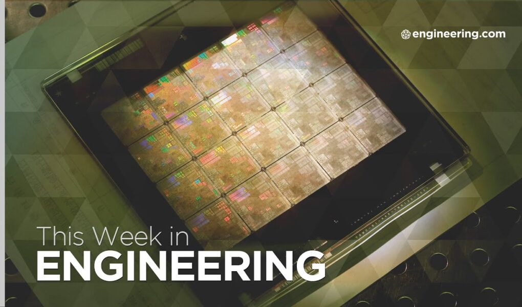
As applications for artificial intelligence are developing rapidly, the need for ever higher computational power to train massive datasets for AI puts a premium on chipmaking technology. Conventional photolithography is increasingly difficult as gate density increases on modern semiconductors, and single digit nanometer devices are more time-consuming and difficult to fabricate.
NVIDIA has developed a software package in collaboration with ASML, Synopsys and TSMC which is designed to run with Nvidia graphics processor units in a system that promises to eventually produce an order of magnitude faster wafer production. 2 nm devices are under study, which may represent the physics limit to PLC development with photolithography technology.
* * *
STEM GAMES:
Play some fun engineering-based STEM games on engineering.com:
https://www.engineering.com/resources/games
* * *
ENGINEERING.COM TV:
Watch in-depth engineering videos made for the engineering professional and found exclusively on engineering.com TV:
For the Design Engineer: https://www.engineering.com/viewAll?category=designing-the-future
For the Manufacturing Engineer: https://www.engineering.com/viewAll?category=manufacturing-the-future
* * *
#NVIDIA #AI #photolithography
Source


Please, where will they get their Neon ?